Material for future electronics: New method makes graphene nanoribbons easier to produce
.png)
Russian researchers have proposed a new method for synthesizing high-quality graphene nanoribbons — a material with potential for applications in flexible electronics, solar cells, LEDs, lasers, and more. Presented in The Journal of Physical Chemistry C, the original approach to chemical vapor deposition, offers a higher yield at a lower cost, compared with the currently used nanoribbon self-assembly on noble metal substrates.
Silicon-based electronics are steadily approaching their limits, and one wonders which material could give our devices the next big push. Graphene, the 2D sheet of carbon atoms, comes to mind but for all its celebrated electronic properties, it does not have what it takes: Unlike silicon, graphene does not have the ability to switch between a conductive and a nonconductive state. This defining characteristic of semiconductors like silicon is crucial for creating transistors, which underlie all of electronics.
However, once you cut graphene into narrow ribbons, they gain semiconducting properties, provided that the edges have the right geometry and there are no structural defects. Such nanoribbons have already been used in experimental transistors with reasonably good characteristics, and the material’s elasticity means the devices can be made flexible. While it is technologically challenging to integrate 2D materials with 3D electronics, there are no fundamental reasons why nanoribbons could not replace silicon.
A more practical way to obtain graphene nanoribbons is not by cutting up graphene sheets or nanotubes but the other way around, by growing the material atom by atom. This approach is known as bottom-up synthesis, and unlike its top-down counterpart, it yields structurally perfect, and therefore technologically useful, nanoribbons. The currently dominant method for bottom-up synthesis, known as self-assembly, is costly and difficult to scale up for industrial production, so materials scientists are seeking alternatives to it.

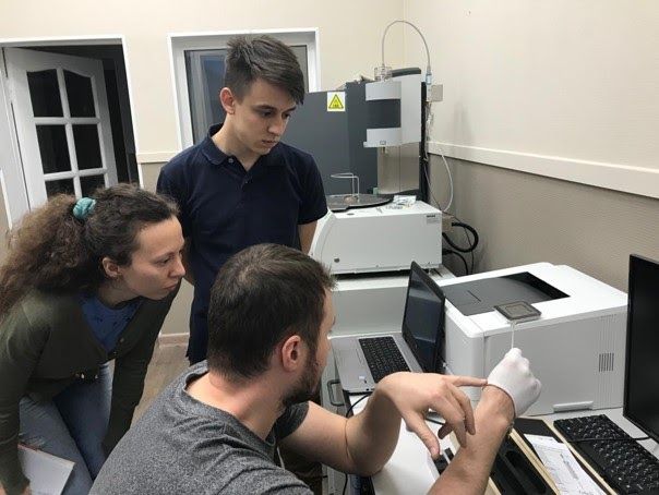
Photo. Researchers operating a NETZSCH Jupiter thermal analyzer in the MIPT Laboratory of Nanocarbon Materials. Courtesy of the researchers
“Graphene nanoribbons are a material whose properties are of interest to fundamental science and hold a promise for applications in all sorts of futuristic devices. However, the standard technique for its synthesis has some drawbacks,” explained Pavel Fedotov, a senior researcher at the MIPT Laboratory of Nanocarbon Materials. “Maintaining ultrahigh vacuum and using a gold substrate is very costly, and the output of material is comparatively low.”
“My colleagues and I have proposed an alternative way to synthesize atomically flawless nanoribbons. Not only does it work under normal vacuum and with the much cheaper nickel substrate, the yield increases by virtue of the nanoribbons being produced as multilayer films, rather than individually. To separate these films into monolayer ribbons, they are put in suspension,” the researcher went on. “Importantly, none of that compromises the quality of the material. We confirmed the absence of defects by obtaining the appropriate Raman scattering profiles and observing photoluminescence of our nanoribbons.”
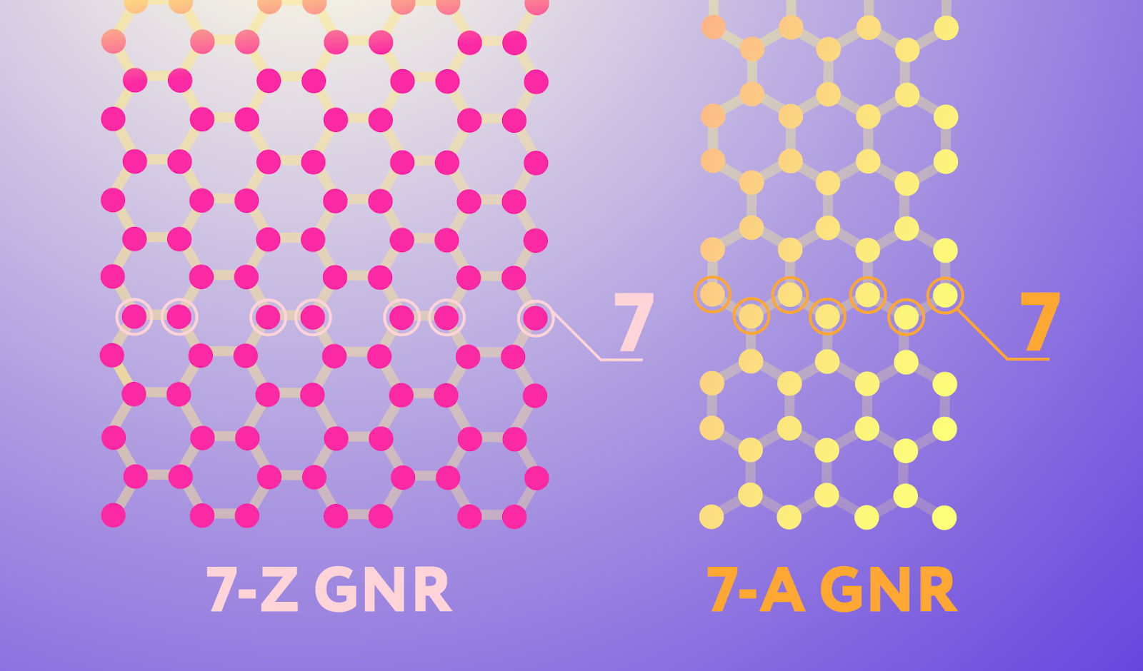
Graphene nanoribbons come in different types, and the ones that the Russian scientists manufactured using their original chemical vapor deposition technique have the structure depicted on the right in Figure 1. They are seven atoms wide and have edges someone found reminiscent of an armchair, hence the name: 7-A graphene nanoribbons. This type of nanoribbons has the semiconducting properties valuable for electronics, unlike its 7-Z cousin with zigzag edges (shown on the left), which behaves like a metal.

Figure 1. Two nanoribbon edge configurations. The pink network of carbon atoms is a ribbon with zigzag (Z) edges, and the yellow one has so-called armchair (A) edges. Note that while nanoribbons come in many different widths, the ones in the image are by convention both considered to be seven atoms wide. Credit: Daria Sokol/MIPT Press Office
The synthesis occurs in an airtight glass tube evacuated to one-millionth the standard atmospheric pressure, which is still 10,000 times higher than the ultrahigh vacuum normally required for nanoribbon self-assembly. The initial reagent used is a solid substance containing carbon, hydrogen, and bromine and known as DBBA. It is placed in the tube with a nickel foil, pre-annealed at 1,000 degrees Celsius to remove oxide film. The glass tube with DBBA is then subjected to heat treatment for several hours in two stages: first at 190 C, then at 380 C. The first heating leads to the formation of long polymer molecules, and during the second stage, they transform into nanoribbons with atomically precise structure, densely packed into films that are up to 1,000 nanometers thick.
After obtaining the films, the researchers suspended them in a solution and exposed them to ultrasound, breaking up the multilayer “stacks” into one-atom-thick carbon nanoribbons. The solvents used were chlorobenzene and toluene. Prior experiments showed these chemicals to be optimal for suspending nanoribbons in a stable manner, preventing aggregation back into stacks and the appearance of structural defects. Nanoribbon quality control was also done in suspension, via optical methods: The analysis of Raman scattering and photoluminescence data confirmed that the material had no significant defects.
Because the new synthesis technology for manufacturing defectless multilayer 7-A carbon nanoribbons is comparatively cheap and easy to scale up, it is an important step toward introducing that material into the large-scale production of electronic and optical devices that would eventually vastly outperform the ones existing today.
“Experience shows that once a new carbon material is discovered, that means new properties and new applications. And graphene nanoribbons were no different,” the head of the MIPT Laboratory of Nanocarbon Materials, Elena Obraztsova recalled. “Initially, nanoribbons were synthesized inside single-walled carbon nanotubes, which served to constrain ribbon width. It was on these embedded nanoribbons that luminescence was originally demonstrated, with its parameters varying with nanotube geometry.”
“Our new approach — bottom-up chemical vapor deposition — enables ultranarrow graphene ribbons to be produced in large amounts and under fairly mild conditions: moderate vacuum, nickel substrate. The resulting material exhibits bright excitonic photoluminescence. It is promising for many applications in nonlinear optics, which we are going to pursue,” the researcher added.
The study reported in this story featured researchers from MIPT, Prokhorov General Physics Institute and the Institute of Bioorganic Chemistry of the Russian Academy of Sciences, the Russian Quantum Center, Skoltech. That research was supported by the Russian Foundation for Basic Science grant Nos. 19-32-60006 and 18-29-19113_mk.
___
The Laboratory of Nanocarbon Materials was established at MIPT in 2018 under Project 5-100, basing on the Laboratory for Nanomaterial Spectroscopy of Prokhorov General Physics Institute. Headed by Elena Obraztsova, the MIPT laboratory focuses on low-dimensional carbon material synthesis, research, and applications. Besides the more familiar graphene and single-walled carbon nanotubes, the lab investigates new modifications of these materials: doped graphene, graphene nanoribbons, as well as nanotubes filled with donor and acceptor inclusions. The team of the laboratory has worked out and published recommendations on the application of nanomaterials as saturable absorbers in laser physics, conductive transparent electrodes in optoelectronics, as well as in plasmonic terahertz interferometry.
___
Header Image. Presenting a new efficient method for nanoribbon manufacture. Credit: Daria Sokol/MIPT Press Office